Electronics Manufacturing Services
From board fabrication and assembly to engineering support and turnkey EMS delivery, ULIKE keeps manufacturing review, testing and handoff in one controlled workflow.
Services
Provide complete electronics manufacturing solutions for customers.
PCB
PCBA
CAD
EMS
Hardware Innovation Design
Vertical integration solutions for customer product R&D and technology innovation.
Manufacturing Integration Service
Technology chain + supply chain + flexible factory.
Service catalog
Choose the service entry that best matches your current engineering or delivery stage.
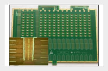
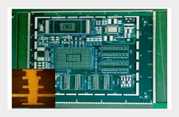
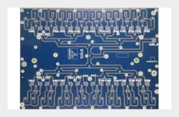
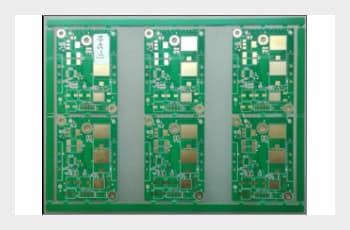
PCB Fabrication
High-precision multilayer boards, rigid-flex boards, HDI boards, high-frequency boards, metal substrates, and thick copper boards.
View details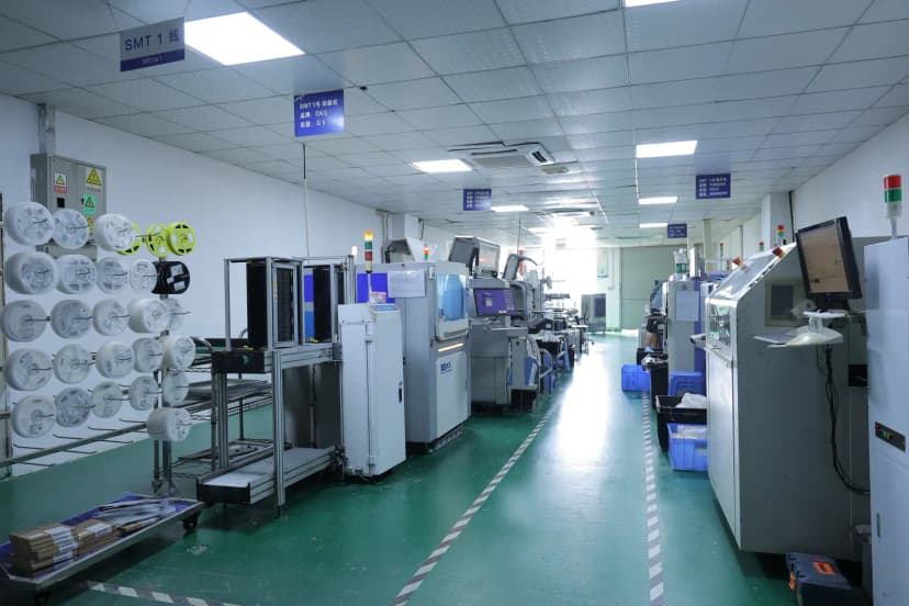
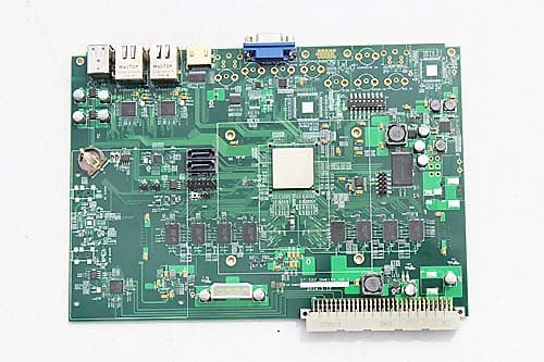
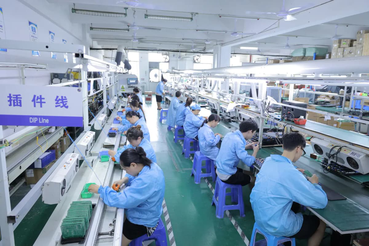
PCBA Manufacturing
Prototype and batch PCBA production with SMT placement, DIP soldering, BGA processing, conformal coating, testing, and packaging.
View details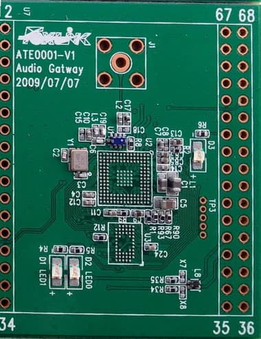
CAD Engineering
High-speed PCB layout, signal integrity planning, EMC improvement, footprint library support, and design-for-manufacturing review.
View details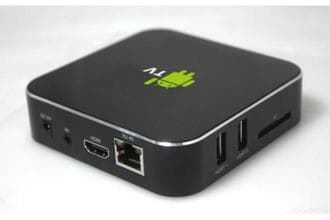
EMS Turnkey Delivery
Hardware development, component sourcing, assembly, testing, finished product integration, plastic tooling, and logistics coordination.
View detailsPCB options
Based on your business attributes, we provide more possibilities.
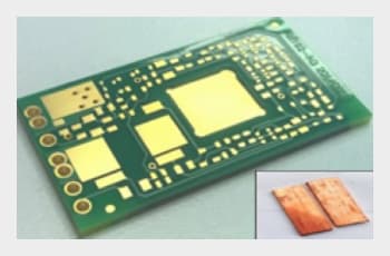
High Multilayer Board
24L, board thickness 5.0mm, minimum line width / spacing 4.0mil / 4.0mil.
HDI Board
16L, board thickness 2.5mm, minimum line width / spacing 3.0mil / 3.0mil.
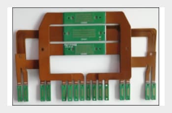
Rigid-Flex Board
14L, board thickness 3.5mm, minimum line width / spacing 8.0mil / 8.0mil.
High-Frequency Board
Material: Ro4730G3, 3L, board thickness 2.0mm.
Metal Substrate
8L / 5.0mm, copper substrate thickness 3.0mm, minimum line width / spacing 10.0mil / 8.0mil.
Thick Copper Power Board
4L, board thickness 1.2mm, minimum line width / spacing 7.0mil / 4.6mil.
Technology and Engineering
ULIKE focuses on professional service, punctuality and trustworthiness, providing integrated solutions for customers.

Technical Capability
Stable placement production for 300-450 product projects. Maximum PCB size: 600x320mm; minimum PCB size: 50x50mm; PCB thickness: 0.4-5mm; component range: 0201-150mm; maximum placement height: 25mm; minimum lead pitch: 0.3mm; minimum ball pitch: 0.4mm; minimum placement accuracy: +/-0.03mm. Laser stencil processing can reach 5 micron precision.
R&D Strength
Fast delivery: double-sided quick-turn boards can be completed within 24 hours, and multilayer quick-turn boards in 2-4 days. Prototype and small-batch advantages support monthly delivery of more than 500 varieties, covering high-layer backplanes, HDI, high-frequency, high-TG, rigid-flex, metal substrates and IC carrier boards.
Quote preparation
A practical checklist for PCB, PCBA, CAD engineering and EMS turnkey projects.
Engineering package
Gerber / PCB file / BOM and approved alternatives / Assembly drawing and coordinates / Mechanical or enclosure limits
Manufacturing route
PCB fabrication only / SMT + DIP assembly / Programming and functional testing / Finished product assembly
Commercial details
Prototype or batch quantity / Target lead time / Packing and logistics notes / Export or domestic delivery address