Case Detail
Review project context, process notes, delivery attention and image records for this case.
PCB Design Cases
Layered PCB Stack-up Design
Layered PCB Stack-up Design is a ULIKE PCB engineering reference. It covers schematic review, PCB layout, stack-up planning, impedance-aware routing, manufacturability review, and engineering documentation.
Ask About Similar Projects- CategoryPCB Design Cases
- Project date2011-4-8 8:53:41
- Image records12
Process notes
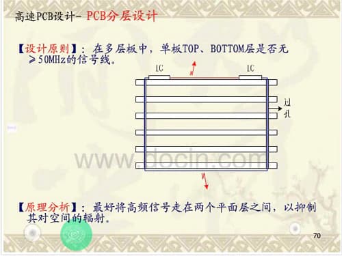
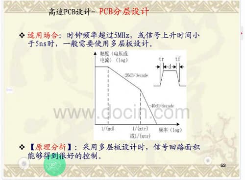
- multilayer PCB design is usually recommended when clock frequency exceeds 5 MHz or signal rise time is below 5 ns
- PCB design and engineering reference
- Layout, stack-up, impedance, and manufacturability review
- Prototype and quick-turn production support
- Engineering documentation for PCB and PCBA handoff
Delivery attention
- Provide mechanical limits, connector positions and keep-out areas before layout starts.
- Confirm stack-up, impedance and key signal requirements early to reduce board revision.
- Before fabrication, review Gerber, drill, paste mask and assembly drawings together.
Project record
ULIKE used this PCB engineering case to support manufacturable layouts, clearer production documentation, faster prototype cycles, and smoother handoff into PCB or PCBA production. Key technical notes include: multilayer PCB design is usually recommended when clock frequency exceeds 5 MHz or signal rise time is below 5 ns; PCB design and engineering reference; Layout, stack-up, impedance, and manufacturability review; Prototype and quick-turn production support.
The work is suitable for customers that need reliable engineering review, production control, quality verification, and delivery handoff.
Image record
Photos are kept as production and project references.