Case Detail
Review project context, process notes, delivery attention and image records for this case.
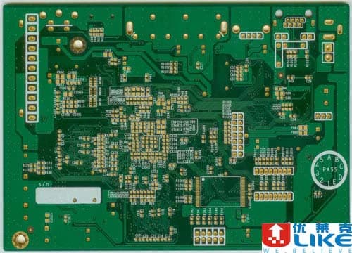
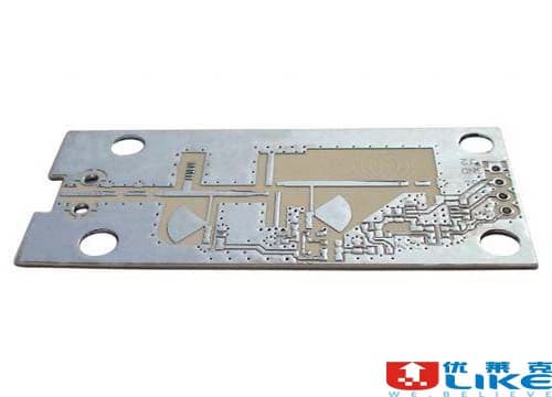
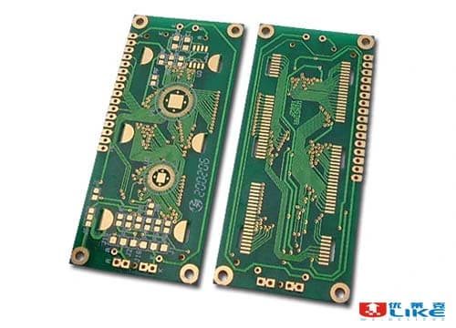
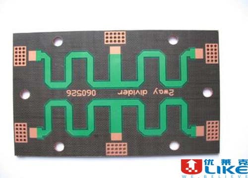
PCB Design Cases
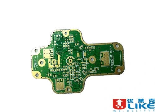
4.00mm Special-shaped PCB Board
4.00mm Special-shaped PCB Board is a ULIKE PCB engineering reference. It covers schematic review, PCB layout, stack-up planning, impedance-aware routing, manufacturability review, and engineering documentation.
Ask About Similar Projects- CategoryPCB Design Cases
- Project date2011-4-8 8:53:41
- Image records6
Process notes
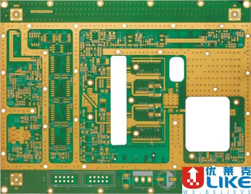
- special-shaped TG170 8-layer PCB
- 2-10 layer multilayer boards in volume, with small-batch 6-layer and 8-layer HDI support
- minimum line width / spacing: 3 mil / 3 mil; BGA pitch around 0.25 mm
- minimum finished hole diameter: 0.1 mm
- maximum board size: 610 mm x 1200 mm
- solder mask inks: Tamura and Taiyo photosensitive inks
Delivery attention
- Provide mechanical limits, connector positions and keep-out areas before layout starts.
- Confirm stack-up, impedance and key signal requirements early to reduce board revision.
- Before fabrication, review Gerber, drill, paste mask and assembly drawings together.
Project record
ULIKE used this PCB engineering case to support manufacturable layouts, clearer production documentation, faster prototype cycles, and smoother handoff into PCB or PCBA production. Key technical notes include: special-shaped TG170 8-layer PCB; 2-10 layer multilayer boards in volume, with small-batch 6-layer and 8-layer HDI support; minimum line width / spacing: 3 mil / 3 mil; BGA pitch around 0.25 mm; minimum finished hole diameter: 0.1 mm.
The work is suitable for customers that need reliable engineering review, production control, quality verification, and delivery handoff.
Image record
Photos are kept as production and project references.